Micro-, nano- and quantum technology infrastructure
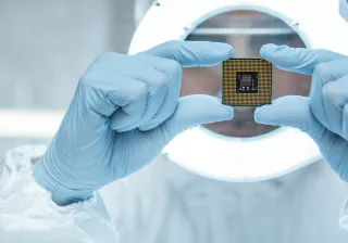
Advanced micro- and nanoelectronics along with photonics and quantum technologies are at the core of tomorrow’s technology. VTT’s world-class technology infrastructure enables material development, device development, concept creation, innovation, design, prototyping, piloting, fabrication and characterisation of micro- and nanoelectronic components.
At VTT, we are our customers’ partners from the early innovation stage all the way to small-scale manufacturing and technology transfer. Our experts help you develop next-generation solutions and bring them to market. Our IP is available for licensing, and we have a wide network of collaboration companies to support technology transfer to high volume production as well as capabilities to integrate software and AI to products.
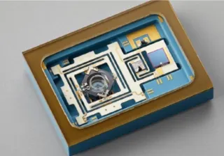
VTT’s micro- and nanoelectronics technology infrastructure supports the entire research and development cycle of technologies such integrated photonics, MEMS, quantum, superconducting technologies, 3D integration, post-CMOS processing, 2D materials, RF, piezo materials as well as semiconductor technologies. Our processing capabilities also allow you to make material development for specific applications.
Our key infrastructure
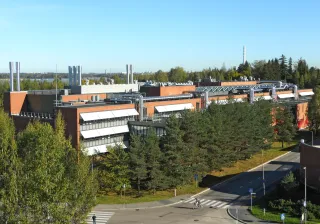
- Our technology infrastructure is located in Micronova, Espoo, and the coming Kvanttinova hub.
- We support 200 mm wafer size, and in the future we will have 300 mm capabilities.
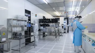
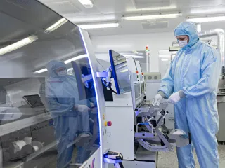
- VTT’s microelectronics cleanroom in Micronova is currently the largest R&D cleanroom in the Nordic countries.
- In-house processing capabilities for semiconducting, integrated photonics, MEMS, post-CMOS, quantum and superconducting technologies.
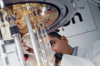
- Extensive sensor development and characterisation laboratories, along with photonics and optics characterisation laboratories.
- Cryogenic characterisation laboratories for the characterisation of superconducting devices and wafer level cryogenic probing.
- ESA external laboratory on millimeter wave technologies, MilliLab.
- We support wafer-level testing and probing facilities.
Cleanroom characteristics
Micronova cleanroom holds the ISO 9001:2015 certification for research and development work and pilot manufacturing for devices for micro-, nano-, photonics and quantum technology applications, wafer processing services and facility maintenance.
Micronova’s cleanroom is run by dedicated maintenance, process engineering, quality and cleanroom operations professionals.
- Total Area 2,600 m2
- Cleanroom Classification ISO 4…ISO 6
- Temperature 21 °C ± 0,5 °C
- Relative humidity 45 % ± 5
- Clean bay – Service chase type
- Raised perforated floor
- Subfab with technical support areas
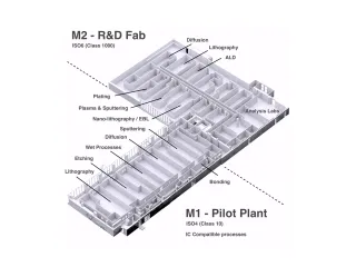
Micronova processing capabilities in 200 mm
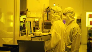
Lithography
- i-line stepper, 5:1, 0.35 µm CD
- DUV KrF stepper, 150 nm CD*
- Automatic CD and defect measurement
- CD-SEM 200/300 mm*
- Contact/proximity aligners
Etching
- Polysilicon/nitride
- Oxide; thin film and advanced oxide etching
- Metals; Al, Mo, Ti-W, Nb (TCP)
- Oxide + metal etch 200 mm*
- Deep silicon etching
- Anhydrous HF vapour
- XeF2 etching
- Ion trimming
- Wet etching, various
Deposition
Seven sputtering tools and multiple evaporators; wide range of materials incl. Al, Ti, TiW, W, AlN, ScAlN, Au, Ag
- Additional sputter tools for 200 mm*
- LPCVD of nitride, poly, and oxide (TEOS, LTO)
- PECVD; nitride and oxide
- 200 mm PECVD M2
- ALD: aluminium oxide, titanium oxide, hafnium oxide, zinc oxide, zirconium oxide, TiN, AlN, etc.
- Parylene
Epitaxy
- Silicon and Germanium selective epitaxy*
- MOCVD
Ion implantation
- Medium-current ion implanter; n- or p-type doping of silicon*
Plating, spin-coating
- Cu (via or wiring), Ni, Sn-Ag, Sn-Pb, In-Sn, Au (automated plating stations 200mm)*
- Polyimide
Annealing
- RTA and annealing in different atmospheres
3D integration
- CMP of Si/oxide 200 mm
- Cu CMP 200 mm for TSV and damascene*
- Direct wafer bonding, fusion and thermal compression
- Silicon backgrinding
- Cu TSV grinding*
- Ion trimming
Backend
- Dicing, flip-chip and wire bonding, pick and place
Characterisation
- Various inline and offline characterisation tools, device parameter analyser, network analyser
*) Coming in 2026–2028 through funding from Chips Act Pilot Line projects FAMES, APECS, PIXEurope and NanoIC and Ministry of Economic Affairs and Employment.
We provide:
- Research and development services from concepting to design, prototyping, piloting, fabrication and characterisation
- Application-specific material development
- Heterogeneous integration and wafer-level packaging solutions
- Our facilities in Oulu also support LTCC packaging for RF and photonics applications
- Large IPR portfolio
For:
- Product companies
- Small- and medium sized companies, start-ups, spin-offs
- Semiconductor suppliers
- Semiconductor equipment makers
- Electronics industry
- Telecom industry
- Space & defence industry
- Medical industry
