Technology keeps on evolving. Today, it is possible to productise the most amazing things: artificial intelligence, quantum computers, self-driving cars, wellbeing sensors, just to mention a few. At their core, all these devices have chips and sensors. That is where their intelligence lies.
In semiconductor manufacturing, the wafer size matters. VTT upgraded its cleanroom to support the processing of 200 mm sized wafers – and it won’t be long till we also have 300 mm wafer size available for selected technologies.
Finland has long traditions in the development of specific chip and sensor technologies for e.g. mobile phones, base stations, as well as quantum technologies. Finnish companies, research organisations and universities have been accumulating significant expertise and experience for decades, thanks to shared goals, RDI actions and continuous development of infrastructures. Our global technology position would hardly be that strong without the bold actions taken for breakthroughs in selected technologies.
Semiconductor technology keeps on evolving and wafer size growing
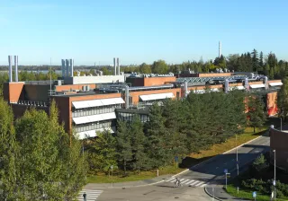
In the past, we only had equipment to process 150 mm sized wafers in Finland. Now VTT’s shared-use cleanroom in Micronova operates equipment converted to 200 mm wafer size. Later, at the new Kvanttinova Hub, VTT will have equipment to support semiconductor manufacturing enabling 300 mm wafer size processing. Why does this matter?
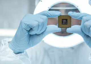
The higher the quantity of specific semiconductor components fabricated on a single silicon wafer, the more profitable the process is – this can save costs and reduce environmental impacts. Digital electronics manufacturing – the most advanced microprocessors in particular – already widely uses the 300 mm wafer size. However, up to the present, specialised microelectronics have been produced in smaller volumes, so the 200 mm wafer size has been sufficient. However, the strong growth of the semiconductor market – especially with artificial intelligence, electric cars, factory automation, new mobile networks and sensor networks becoming more common – will increase demand for specialised microelectronic circuits. The fabs and end users are looking for ways to improve production efficiency, cut costs and reduce environmental load. In this situation, a larger wafer size quickly emerges as an attractive alternative.
Equipment providers put typically most effort on equipment for 300 mm size wafers
For a long time, semiconductor equipment manufacturers have been putting the most effort in developing equipment capable of processing 300 mm size wafers. Equipment reaching the highest processing quality is largely found in the 300 mm wafer range. To be able to develop the most up-to-date technology, companies and research institutes must have access to such high-end equipment already in the research and development phase, as processing equipment for different wafer sizes may produce different results.
In particular, equipment providers are investing in the development of 300 mm wafer size equipment, generally providing them with the latest features. Furthermore, processing 300 mm wafers is more environmentally and resource efficient than processing on smaller wafer sizes.
To be able to develop the latest critical technologies with the latest hardware, the 300 mm processing capability is vital for Finland. Otherwise, others will pass us while we are still stuck on developing older generation technologies.
In specialised microelectronics, converting from 200 mm to 300 mm wafers is a clear technological transformation point. Europe does not yet have access to the kind of semiconductor piloting capabilities in 300 mm wafer size that would support new computing methods and telecommunications, superconducting quantum technology, MEMS sensors and dual-use products.
Finland now has a unique opportunity to boldly advance at the forefront and ensure the growth of the industrial and semiconductor ecosystem in these sectors. By being among the first to develop and utilise the latest technologies in specialised microelectronics, we are laying a strong foundation for future economic growth.
Let’s develop what others do not yet have
We are currently in the fortunate situation to have also technological competencies others do not have. Our strengths include chip design, RF technologies and telecommunications, MEMS sensors, superconducting quantum technology, atomic layer deposition and photonics. This is important because we also need critical technologies developed in other countries – technologies of the kind that we cannot produce or even design ourselves. The most advanced processor technologies are a good example of this. They can only be mass-produced in Taiwan, where an entire nation has been making determined investments in developing the latest semiconductor technologies for decades. Machines can always be moved elsewhere, but it is more difficult to duplicate competence and experience.
With the help of a 300 mm manufacturing line for specialised microelectronics, we will build the conditions for ourselves to be among the developers of the latest critical technologies – of the kind that others do not yet have.
Our aim is to increase the production capabilities of 300 mm size wafers through the European Chips Act 2 to promote and ensure European self-sufficiency and economic growth. In addition to public investments, we need private investments to build and maintain infrastructure. That is why we want to collaborate closely with domestic and European companies to achieve common goals.
