Emerging energy-efficient microelectronics are essential for advancing the digital society, but their development must balance technical performance with environmental sustainability from the earliest stages of research and development. VTT scientists who are developing next-generation technologies to support our digital society take a look at the topic in this blog.
Read the summary
- While advancing semiconductor technology offers significant benefits, it poses environmental challenges due to the intensive resource use and reliance on critical raw materials in manufacturing.
- Developing sustainable semiconductor technologies involves balancing performance with environmental considerations early in R&D, focusing on lifecycle, materials, design and efficient fabrication methods.
- Trade-offs in technologies like RF communication, computing methods and power electronics are explored, highlighting opportunities to reduce environmental impact by optimising material use and enhancing energy efficiency.
This summary is written by AI and checked by a human.
The outlook for the semiconductor industry is positive. According to BCC Research, the global semiconductor chip market is expected to grow from USD 737.2 billion in 2025 to USD 1,600 billion by 2030, representing a compound annual growth rate (CAGR) of 16.1% over the 2025–2030 period. This growth is primarily driven by increasing demand for computing power required for data processing, artificial intelligence and connectivity. Additionally, the continued digitisation of consumer electronics, industrial equipment and vehicles further supports market growth.
Ongoing advancements in semiconductor technology are focused on improving power efficiency and miniaturisation. The developing digital society is dependent on perpetual connectivity and continuous data transfer, increasing computing capabilities and sensing. Energy-efficient operation is a must when the amount of transmitted data increases.
Challenges and trade-offs in sustainable semiconductor manufacturing
But there are serious trade-offs. Semiconductor technology relies on various materials selected for their unique properties and contributions to device performance, including several critical raw materials (CRMs). The manufacturing of integrated circuits is complex and costly, often requiring state-of-the-art manufacturing equipment. Semiconductor fabrication is resource-intensive, consuming significant amounts of energy, water, chemicals and critical raw materials. Semiconductor fabrication contributes to greenhouse gas emissions, climate change, water eutrophication and uses highly poisonous materials.
Product sustainability in the semiconductor industry involves balancing economic advantages with environmental and social benefits. The environmental impact of a product is largely defined during the early phase R&D, making it crucial to consider sustainability from the beginning of the development.
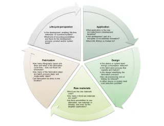
Environmental sustainability can be considered in early-phase microelectronics R&D on five different levels: lifecycle perspective, which application technology is developed for, design choices, raw materials, fabrication aspects and the lifecycle perspective (Konstari, P., & Valkokari, K. (2025). Integration of multi-disciplinary environmental sustainability aspects into early-phase microelectronics research and development. Discover Sustainability, 6(1), 1089.) When developing next-generation microelectronics, researchers must carefully choose materials, layout, fabrication and testing methods. Each decision affects energy use, technical performance, material consumption and environmental impact. These factors should be thoroughly evaluated to minimise environmental harm, while meeting technical performance requirements, in order to allow the development of our digital society.
Next, we explore the trade-offs for three different technologies
Trade-offs for communication technologies
The shift to 6G facilitates advanced services such as autonomous vehicles, smart cities and remote healthcare, requiring solutions capable of transferring more data with less energy. In the congested RF spectrum, RF BAW filters are vital for ensuring signal quality and integrity. The filters must operate at higher frequencies with greater efficiency, while network infrastructure demands smaller, mass-produced filters with high power handling capacity, enabling wider data bandwidths and reduced energy consumption per bit.
RF amplifiers, another essential component, benefit from new materials like wide bandgap (WBG) semiconductors, which improve the energy-efficiency of the devices. Using WBGs on silicon instead of bulk WBG wafers, reduces the amount of critical raw materials (CRMs) required per device. Use of WBG devices reduces the need for bulky passive components (like heat sinks and filters), indirectly lowering the overall material footprint of electronics systems.
As these technologies mature, there is the potential to optimise designs and materials to lower environmental impact, such as replacing CRMs like scandium without compromising performance.
Trade-offs for new computing methods
With recent shifts in computing paradigms, including AI, innovative architectures, such as in-memory and neuromorphic computing, will be required to be able to continue reducing chip energy consumption. These approaches minimise data transfer between memory and processing units, and when combined with novel electrical devices with programmable resistances, it can lower the power use and environmental impact by several orders of magnitude. These novel devices can be processed using non-CMOS materials directly on top of CMOS wafers for an embedded solution. Although these advanced post-CMOS technologies increase the complexity of fabrication and rely on more critical raw materials, the use of nm-thick layers means that very small amounts are consumed, and the resulting efficiency gains in the application can justify their use. For maximizing impact, ongoing R&D should continue to seek ways to reduce critical material usage and chip size without compromising performance, while also improving manufacturing maturity and yield.
Trade-offs for power electronics and sustainable mobility
The shift to electric vehicles (EVs), and the adoption of electric motor systems in industry are driving advances in power electronics, particularly through wide bandgap (WBG) semiconductor technologies like gallium nitride (GaN) and silicon carbide (SiC). These materials enable more efficient, compact and reliable power converters by offering better electrical performance and thermal management. In EVs, WBG devices improve battery life and driving range by reducing power losses. Their integration also supports sustainable transport and industrial automation. Development efforts focus on cost-effective manufacturing, optimised use of critical raw materials and eco-design strategies such as recyclability and lifecycle efficiency. System-level innovations in packaging, thermal management, and control algorithms facilitate the deployment of smart grids and renewable energy integration. While full lifecycle understanding of WBG devices in these new applications is still limited, current research seeks to establish clear sustainability metrics for these emerging technologies.
Balancing between manufacturing and performance requirements
Emerging technologies enable the development of our digital society. However, the environmental impact of semiconductor manufacturing must be balanced with the performance requirements. Emerging technology development is first and foremost performance. When the technology becomes more mature, optimisations of designs, systems and materials gain more attention. Nevertheless, it is important that different environmental sustainability aspects are identified and evaluated already in early-phase R&D and possibilities for alternative technologies are considered. In addition to the operational optimisation of the fabrication, aspects related to raw materials, the design, the lifecycle perspective and the application itself can be discussed and considered already in early-phase R&D.
Writers
- Piia Konstari, Director, Microfabrication services
- Pekka Pursula, Director, Microelectronics and quantum technology research
- Karl-Magnus Persson, Senior Scientist, Specialist in neuromorphic devices
- Sami Suihkonen, Specialist in WBG semiconductor technology
- Tuomas Pensala, Research Team Leader, Principal Scientist, Specialist in RF filters
