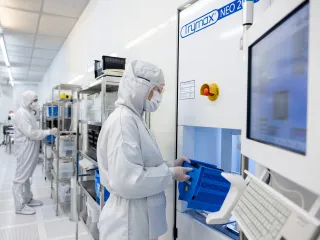
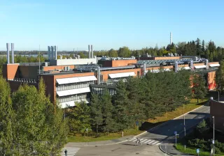
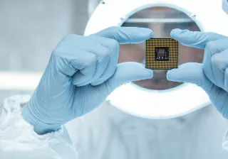
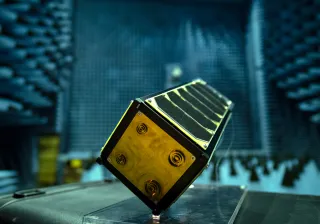
Kyocera Technologies relies on VTT’s shared cleanroom facilities to design and refine high-precision MEMS timing resonators. The unique microfabrication environment and piloting capabilities in Micronova help companies grow within Finland’s world-leading microelectronics ecosystem.
Key facts
Investing in their own cleanroom infrastructure is often too expensive for microelectronics startups and SMEs such as Kyocera Technologies.
VTT’s shared-use cleanroom has offered Kyocera Technologies access to state-of-the-art equipment, maintenance expertise and a scalable operating model.
Advanced microfabrication and piloting services have helped the company in solving both the theoretical and practical challenges to enable future electronics.
Kyocera Technologies is one of the global leaders in MEMS (micro-electromechanical systems) resonator research and development for the global timing and frequency control market. Originally a VTT spinoff, the company has since grown into a MEMS Centre of Excellence, located next to Micronova in Otaniemi, Finland.
The company is on a quest to make smart devices and wearables even smarter, smaller, more durable and precise. Its parent company Kyocera Group is a multinational manufacturer of high-tech ceramics, electronic components, solar cells and office equipment.
Building equivalent capacity ourselves would have required investing tens of millions of euros.
Building Europe’s capacity in specialised microelectronics
The global semiconductor industry continues to surge, driven by increased demand for connectivity, highly integrated systems and AI. In this context, specialised microelectronics – such as MEMS, RF and quantum devices – are becoming critically important. Europe, striving for strategic technological sovereignty, is strengthening its capacity in these domains.
Finland’s microfabrication and piloting capabilities are central to that effort. At the heart of it is VTT’s Micronova cleanroom in Otaniemi, serving as a multi-user R&D hub. Through shared infrastructure, emerging companies can innovate on industrial-grade tools without the burden of investing in their own facilities. This makes the Finnish ecosystem a magnet not only for research, but also for forward-looking deep-tech companies such as Kyocera Technologies.
Having these capabilities and infrastructure available right next door to our offices in Otaniemi is a major asset for us.
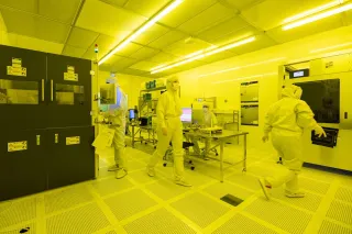
Industrial-grade infrastructure enables rapid iteration and collaboration
Besides advanced design and simulation, developing MEMS-based timing resonators demands access to high-end cleanroom processing equipment, precise toolsets and prototyping capability. For a small company, replicating this infrastructure is prohibitively expensive.
“You could say we wouldn’t exist without access to VTT’s industrial-grade cleanroom facilities. Building equivalent capacity ourselves would have required investing tens of millions of euros,” says Kyocera Technologies’ Managing Director Tapio Sulkava.
He emphasises the value of a shared history and close cooperation with VTT in creating a strong working culture.
“We have made a strategic choice to partner with VTT. Having these capabilities and infrastructure available right next door to our offices in Otaniemi is a major asset for us. Also, as one of the main users of the cleanrooms, we have developed a kind of mutual understanding so that we always find solutions to any technical challenges that may occur,” Sulkava says.
A unique shared-use model supported by world-class expertise
Benefits provided to Kyocera Technologies through its cooperation with VTT include:
Flexible access to advanced tools and expertise
Accelerated product development and prototyping
Growth opportunities within Northern Europe’s strongest microelectronics ecosystem.
Piia Konstari, VTT’s Director of Microfabrication Services, highlights how VTT’s shared-use model provides customers access to a wide range of processing capabilities under one roof.
“VTT manages the maintenance of the cleanroom and its equipment and provides processing support and extensive R&D services for companies. Our cleanroom organisation, with more than 40 experts, takes even better care of the reliable maintenance of equipment and processes than research infrastructures in general,” Konstari points out.
VTT recently completed a major conversion of its cleanroom in Micronova from 150 mm to 200 mm silicon wafer capacity. This was not just a technical upgrade – it strategically aligns with industry-standard wafer sizes used, for example, in MEMS devices.
Oliver Pabst, Head of Fab Operations at VTT, emphasises: “By converting to 200 mm, we've significantly enhanced our toolset. Now we can support process flows that mirror industrial manufacturing, lowering the gap between R&D and pilot production.”
Kvanttinova expands Finland’s lab-to-fab pathway
Kyocera Technologies’ long-term growth is bolstered by plans for the Kvanttinova ecosystem, a new piloting and development hub for microelectronics and quantum technologies. The Kvanttinova initiative, backed by VTT, Aalto University, the City of Espoo and industry players, will offer lab-to-fab capacity and further fabrication capabilities. As Kyocera Technologies scales, it can smoothly transition into these next-phase facilities.
“I expect Kvanttinova to accelerate the positive spiral generated by the Micronova hub, with further investments coming in and companies joining the community. Also, I believe VTT has gained valuable experience and feedback from users such as us on how to develop the ecosystem so that it provides stronger capabilities also for the manufacturing stage,” Sulkava concludes.
