Integrated photonics

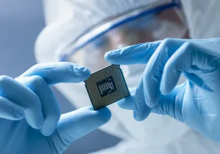
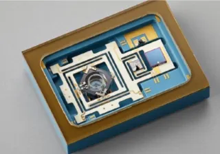
Our integrated photonics solutions combine optical components and functions onto a single chip, enabling small footprint, high performance and low loss. From simple photonic sensors to complex systems like photonic computing and optical communication, our innovative approach integrates waveguides, photonic integrated circuits (PIC), modulators and lasers into semiconductor platforms.
VTT’s integrated photonics solutions offering
Our integrated photonics solutions enable the integration of optical systems into a small footprint (such as a single chip), promoting cost and power efficiency.
We offer low-loss specific photonic integrated circuits for highly efficient transmission and processing of optical signals with minimal signal degradation.
Photonic integrated circuits for various fields: data communications, sensing applications, LiDAR, medical, spectroscopy, quantum, 6G, wearable sensors, optical switching, and RF.

Why integrated photonics?
Small optical chips can efficiently control and manipulate light, making it possible to create compact, low-power and high-performance optical systems. They enable a wide range of applications and have the potential to revolutionise various fields, from communications and computing to healthcare and environmental monitoring.
Benefits include:
- Miniaturisation of optical components and systems allows compact and portable devices.
- Integrating different optical components onto one chip simplifies manufacturing, improves resource efficiency, and boosts overall system performance.
- Enhanced bandwidth capabilities, essential for data-intensive applications like data communications and high-performance computing.
- Especially at high frequencies, photonics-based signal transmission consumes much less energy than electronic transmission.
Why choose VTT for integrated photonics solutions?
There are several factors that make us an optimal candidate for your integrated photonics R&D. Here are a few of them:
- We offer a unique combination of low loss and ultra-broadband capabilities in optical wavelengths. This makes our solutions applicable across a range of applications and boosts efficiency, bandwidth, data transfer rates and systems reliability.
- Our PIC technology shrinks optical system size from tens of centimetres to a few millimetres.
- Large and licensable IP portfolio for photonic integrated circuits.
- Cost-efficient path from design to proof of concept.
- VTT has an extensive heritage in developing integrated photonics solutions. We’ve been creating innovative optical waveguide devices for various high-end applications since the 90s.
- World-class expertise meets agility and customisability. VTT’s tailored offerings provide exactly the integration photonics solution you need. Our experts can design and simulate device configurations precisely aligned with specific application requirements, from specialised research prototypes to scalable production.
Full range of services across the entire value chain
Whatever your goals, our experts can assist you every step of the way, including:
- Designing and simulating device configurations
- Fabricating prototypes in our state-of-the-art clean room facility
- Conducting testing to ensure optimal device performance
- Packaging services to seamlessly integrate your device into the final product
- Support for early-stage manufacturing
- Scaling production by identifying suitable manufacturing partners and providing tech transfer services and IP licensing.
VTT offers heterogeneous, hybrid and monolithic integration
Our integration techniques are tailored to your needs and allow you to combine the benefits of different technologies:
- Monolithic integration, seamlessly merging active and passive components, allowing the incorporation of germanium detectors, modulators and more
- Hybrid integration, including flip-chip bonding, enabling the integration of III-V lasers, amplifiers, and modulators with silicon-on-insulator (SOI) or silicon nitride (SiN) waveguides
- Heterogeneous integration, including graphene integration and wafer bonding, which allows wafer-level processing to continue after the integration of new materials.
Our 3 µm SOI PIC technology has the lowest loss of all densely integrated silicon photonics technologies
Our state-of-the-art passive components offer polarisation-independence and broadband operation at wavelengths ranging from 1.2 to over 3 µm, while propagation losses can reach down to a few dB per metre without compromising integration density.
Integrated photonics with SiN waveguides
Our SiN technology broadens the available wavelength range to visible wavelengths, ideal for many quantum computing and medical applications. Our waveguides offer flexibility with options for various thicknesses, material compositions and waveguide geometries.
We assemble and package PICs
Our assembly labs enable fibre pigtailing with low losses via cutting-edge technologies such as polymer lenses, up-reflecting mirrors, waveguide tapering, anti-reflection coatings and V-groove alignment.
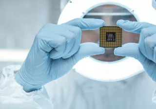
Manufacturing is possible in our dedicated cleanroom facilities. We also have in-house characterisation laboratories.
VTT can also help you with:
- Integrated photonics solutions for LiDAR
- LTCC packaging for harsh environments for photonic chips
- CMOS fabrication
- Quantum computers and signal-feeding
- Optical computing and wideband RF applications like beam steering: replacing multiple microwave cables with a single optical fibre.
See our integrated photonics solutions at work!
Case Rockley Photonics
In 2014–2021, Rockley Photonics was one of the fastest growing companies in the field of integrated photonics. Since the beginning, VTT helped Rockley to develop and prototype their PIC platform. By 2021, the PIC technology was transferred to Rockley and its large-volume foundry partners in order enable the commercialisation of Rockley’s optical sensors in consumer applications.

Related infrastructure
VTT is an integral part of these photonics ecosystems
VTT is a key player in several EU projects
How to work with us on integrated photonics solutions?
From concept to assembly and packing, VTT can kick-start your integrated photonics goals! Get in touch with us now.
Meet our experts


Publications related to integrated photonics
Contact us here!
FAQ – Frequently Asked Questions about integrated photonics solutions
What are integrated photonics solutions?
They combine multiple optical components—like lasers, modulators, detectors, and waveguides - on a single small chip offering high performance and energy efficiency.
What applications does this technology support?
The solutions serve photonic computing, optical data communication, LiDAR, medical diagnostics, spectroscopy, sensing, quantum systems, and 6G networks.
What capabilities does VTT offer?
VTT provides design, simulation, prototyping, cleanroom fabrication, performance testing, assembly, packaging, and support for early-stage manufacturing scale-up.
Why choose VTT for integrated photonics?
VTT excels in low-loss and broadband PICs, photonic chip miniaturisation, an extensive IP portfolio, and integrated design-to-proof-of-concept services.
How does this benefit my product development?
You get compact, low-power optical chips quickly - from concept through to pilot-ready devices - ready for sectors like healthcare, communications, sensing, quantum, or 6G.
This FAQ is written by AI and checked by a human.


