
Microfabrication enables the creation of microelectronics devices that power for example today’s sensing, computing and communication technologies. As the race for technological leadership intensifies, companies face growing pressure to accelerate innovation, validate new concepts efficiently and ensure reliable microelectronics manufacturing. VTT’s microfabrication and piloting services bring together decades of expertise in specialised microelectronics and a state-of-the-art cleanroom infrastructure, supporting you from early research and process development to prototyping, piloting and commercialisation.
Key facts
Bring new products to market faster with VTT’s expertise. We provide services across the entire development cycle – from materials and device R&D, innovation to prototyping, piloting and small-scale fabrication.
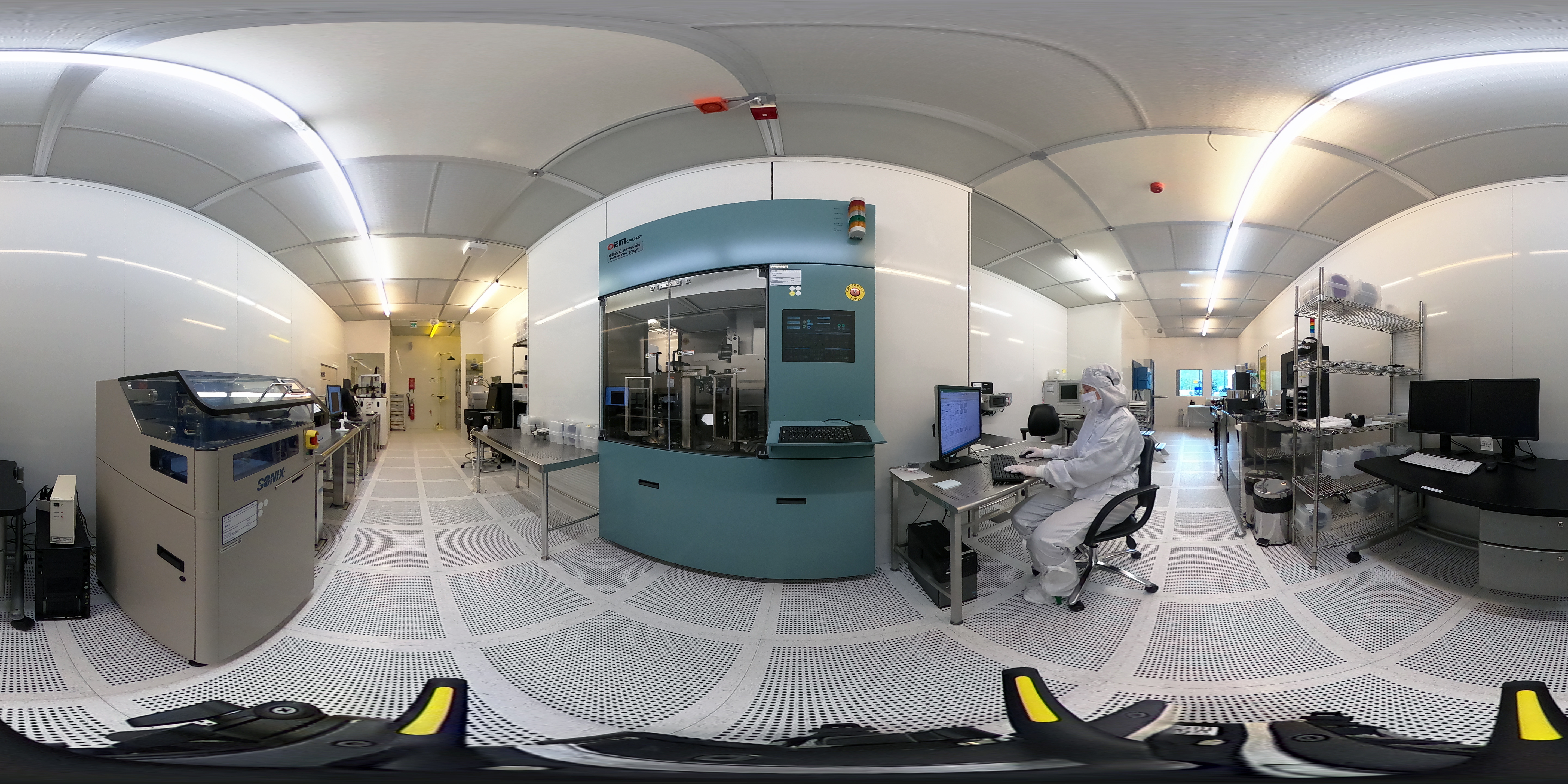
Access our shared cleanrooms in Micronova that enable the fabrication of MEMS, RF, integrated photonics, quantum devices, superconducting devices, post-CMOS processing, as well as power electronics.
Accelerate business growth by licensing VTT’s proven process or device IP.
Semiconductors and the growing need for microfabrication
The global semiconductor market is projected to grow significantly in the coming years, driven by digitalisation, increased consumption of consumer electronics, development of industrial systems and increased fabrication of electric vehicles. This growth is increasing the demand for microfabrication and piloting of innovative devices and systems.
Piloting accelerates innovation and reduces time to market
Working with VTT gives companies access to advanced microfabrication and piloting services. This allows you to reduce overall development costs and shorten time to market. The services enable you to experiment with new designs based on either experimental of piloting processes, driving IP creation and technology development.
We also offer access for companies to our cleanroom and equipment. Our shared microelectronics infrastructure is a sustainable solution allowing multiple users to benefit from the same equipment. When multiple users share the same cleanroom facilities and equipment, overall consumption of energy, electricity, water and materials is optimised. This makes operations more efficient both economically and environmentally, while keeping emissions to a minimum.
Micronova cleanroom facilities

VTT’s microfabrication services
We offer three types of microfabrication services: R&D services, piloting services based on PDKs and equipment access services. These make full use of our key capabilities and enable the design and fabrication of devices across a wide range of technologies.
Our services are for spin-offs, start-ups, SMEs, large companies, RTOs and academia. With us, you get the entire development cycle under one roof – from research and process development to prototyping, piloting and small-scale manufacturing. This integrated approach allows you to turn research into viable products efficiently and sustainably, while tailoring every project to your specific goals.
Key capabilities and supported technologies
Our R&D and innovation activities focus on a wide range of technologies, including MEMS, RF, integrated photonics, quantum technologies, analogue computing, post-CMOS processing, power electronics and materials development for microelectronics.
Through our shared cleanroom facilities at Micronova and the upcoming Kvanttinova, companies can utilise a wide range of 200 mm processing capabilities supporting diverse micro-, nano- and quantum-technology applications. In the future, we will also expand our offering to include 300 mm processing capabilities.
2D materials and post-CMOS integration
- Graphene biosensors
- Ferroelectric non-volatile memories
- Post-CMOS integration
Key processes
- i-line, maskless and EBL lithography
- Cu Damascene and Cu TSVs for BEOL
- Wide range of ALD films
- WLP
Integrated photonics
- Passive and active devices on 3µm SOI platform
- SiN nanoscale SiPh
- Photonic integration for cryogenic applications
Key processes
- KrF DUV and i-line lithography for WG patterning
- SiGe epitaxy for active devices
MEMS
- SOI-MEMS, piezo-MEMS and Surface MEMS devices
- Fabry-Perot interferometers
- Acoustic, gas, particle sensors
Key processes
- LTCC packaging
- Wafer bonding
- CMP
RF
- 5G/6G BAW filters with 7 – 15 GHz frequency range
- Integrated passive devices
- 3D integration & packaging
Key processes
- Piezo stacks w. AlN / ScAlN
- Cu TSVs
- Ion beam trimming
Superconducting technologies
- Superconducting qubits
- Si QD qubits
- Quantum sensing
- Josephson logic
- Cryogenic CMOS
- 3D integration
Key processes
- Trilayer Josephson junctions
- Manhattan qubits
- Superconducting TSV and flip-chip
Power electronics
- Power HEMTs
Key processes
- MOCVD GaN
Related infrastructure


Expanding Finland’s processing capabilities through participation in European pilot lines
VTT is involved in several European Chips JU pilot lines, underlining its central role in the European semiconductor ecosystem and linking the Finnish ecosystem to broader European collaboration. VTT participates in the FAMES, APECS, NanoIC and PIXEurope Chips JU pilot lines.
With funding from the EU, the Ministry of Economic Affairs and Employment and Business Finland, VTT is strengthening Finland’s capability to manufacture specialised chips. New processing capabilities are being procured and existing manufacturing equipment upgraded. These investments enhance Finland’s competitiveness and access to critical technologies and position the country more firmly within the European chip value chain.
The new manufacturing equipment and processing capabilities will be located at VTT’s facilities at Micronova and in the planned Kvanttinova hub in Otaniemi. Both businesses and the wider ecosystem will have access to these new and upgraded processing resources, as well as existing VTT processing infrastructure within the shared Micronova cleanrooms.
Research ecosystem built around cutting-edge infrastructure
VTT plays a key role in Finland’s microelectronics and quantum technology research, development and innovation. VTT is part of OtaNano, Finland's national research infrastructure for micro-, nano-, and quantum technologies, and the upcoming Kvanttinova ecosystem centers around VTT’s technology infrastructures and Aalto University’s research infrastructures.
Many Finnish microelectronics companies have also emerged as spin-offs from VTT or benefit from its shared-use cleanrooms at Micronova.
How to work with us
We collaborate with you at any stage of your journey, from the initial idea to implementation. Every project is unique, and we tailor our approach to your specific needs.
-
Get in touch!
Tell us what you want to achieve, and we’ll explore how to make it happen. After the initial discussion, we propose the most suitable way forward based on your objectives and resources. -
Customised partnership
Our experts work hand in hand with your R&D team, helping you accelerate your innovation process. From lab to fab, our services are at your disposal. We help you fabricate and pilot your designs. Our technology is available for technology transfers to large volume fabs. -
Cooperative projects
We frequently collaborate with business partners and funding agencies in joint research and development projects. -
Networks and ecosystems
We work with companies and research institutions around the world and are happy to put you in touch with the right sparring or development partners.
Contact us here!
Meet our experts

Some questions we can help you with
- How can I access VTT’s microfabrication and piloting services?
- How can I accelerate the development and validation of new devices using advanced microfabrication technologies?
- How can I build on VTT’s existing IP and process expertise to accelerate innovation?


